

Wafer Level Packaging Market Outlook Report Including Segment Analysis and Strategic Industry Insights

The Business Research Company
Wafer Level Packaging Market Overview
The Business Research Company's Wafer Level Packaging Market Outlook Report Including Segment Analysis and Strategic Industry Insights
LONDON, GREATER LONDON, UNITED KINGDOM, October 26, 2026 /EINPresswire.com/ -- "The wafer level packaging market has been experiencing significant growth, driven by rapid advancements in semiconductor technology and increasing demand for smaller, more efficient devices. As industries continue to evolve, this market is set to expand further, supported by emerging trends and widespread adoption across various applications. Here is an overview of the market size, key drivers, regional trends, and future outlook.
Market Expansion and Growth Trajectory of the Wafer Level Packaging Market
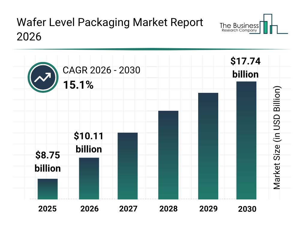
The wafer level packaging market has seen rapid expansion in recent years. It is projected to increase from $8.75 billion in 2025 to $10.11 billion in 2026, achieving a compound annual growth rate (CAGR) of 15.5%. This growth during the historical period stems from the rising demand for compact semiconductor packages, enhanced semiconductor integration, widespread use of portable electronic devices, the need for better electrical performance, and efforts to reduce manufacturing costs.
Download a free sample of the wafer level packaging market report:
https://www.thebusinessresearchcompany.com/sample_request?id=43176000&type=smp&name=Wafer%20Level%20Packaging%20Market%20Report%202026&utm_source=EINPresswire&utm_medium=Paid&utm_campaign=Oct_PR
Looking ahead, the wafer level packaging market is expected to maintain its strong momentum. By 2030, the market size is forecasted to reach $17.74 billion, growing at a CAGR of 15.1%. The factors driving this future growth include increasing demand for high-performance semiconductor devices, broader adoption of advanced heterogeneous integration, growing requirements for compact automotive electronics packages, expanding applications in high-density computing, and a rising need for improved thermal and signal integrity. Notable trends shaping this forecast period include greater acceptance of fan-out wafer level packaging, enhanced use of hybrid bonding technologies, increased interest in three-dimensional wafer level integration, a focus on miniaturized and densely packed structures, and expanded use of wafer-level packaging for heterogeneous integration.
Understanding Wafer Level Packaging and Its Importance
Wafer level packaging is an advanced semiconductor technology that integrates packaging and interconnection processes directly at the wafer stage, prior to chip separation. This method allows the incorporation of protective layers, electrical connections, and miniaturized elements on the wafer itself, resulting in better device performance, smaller package sizes, and more efficient manufacturing. It plays a crucial role in enabling compact, high-performance semiconductor devices by supporting higher integration density, improved signal quality, and simplified production workflows.
View the full wafer level packaging market report:
https://www.thebusinessresearchcompany.com/report/wafer-level-packaging-market-report?utm_source=EINPresswire&utm_medium=Paid&utm_campaign=Oct_PR
Rising Internet of Things (IoT) Adoption Fuels Demand for Wafer Level Packaging
One of the major forces accelerating the wafer level packaging market is the expanding adoption of Internet of Things (IoT) devices. These devices, embedded with sensors, software, and connectivity, gather and share data over the internet. The growing reliance on automation and real-time data collection is driving demand for connected devices that require compact, efficient, and reliable semiconductor solutions. This trend directly supports the increased use of wafer level packaging technologies for next-generation connected gadgets.
To illustrate, in July 2025, the European Commission reported that the number of IoT-connected devices reached approximately 40 billion in 2023 and is expected to rise to 49 billion by 2026, reflecting an annual growth rate of 7%. This surge in connected devices highlights the pivotal role IoT expansion is playing in boosting the wafer level packaging market.
Regional Market Highlights and Future Growth Opportunities
In terms of regional market share, North America held the largest portion of the wafer level packaging market in 2025. However, the Asia-Pacific region is anticipated to experience the fastest growth in the coming years. The comprehensive market analysis includes key areas such as Asia-Pacific, South East Asia, Western Europe, Eastern Europe, North America, South America, the Middle East, and Africa, providing a global perspective on market trends and potential.
What’s new in our 2026 market reports:
• Market attractiveness scoring and analysis
• Total addressable market (TAM) analysis
• Company scoring matrix graphics and tables
• Excel dashboards
• Market hotspots infographics
• Key technologies and future trends
• Updated graphics and tables
Speak With Our Expert:
Saumya Sahay
Americas +1 310-496-7795
Asia +44 7882 955267 & +91 8897263534
Europe +44 7882 955267
Email: marketing@tbrc.info
The Business Research Company - www.thebusinessresearchcompany.com
Follow Us On:
• LinkedIn: https://in.linkedin.com/company/the-business-research-company"
Oliver Guirdham
The Business Research Company
+44 7882 955267
info@tbrc.info
Visit us on social media:
LinkedIn
Facebook
X
Legal Disclaimer:
EIN Presswire provides this news content "as is" without warranty of any kind. We do not accept any responsibility or liability for the accuracy, content, images, videos, licenses, completeness, legality, or reliability of the information contained in this article. If you have any complaints or copyright issues related to this article, kindly contact the author above.
